

Sunday, 19/05/2024 | 05:00 GMT+7
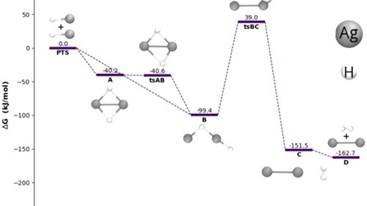
Solar-powered electricity prices could soon approach those of power from coal or natural gas thanks to collaborative research with solar start-up Ampulse Corporation at the U.S. Department of Energy’s (DOE) National Renewable Energy Laboratory (NREL).


 Challenges and Opportunities to promote energy efficiency market in Vietnam
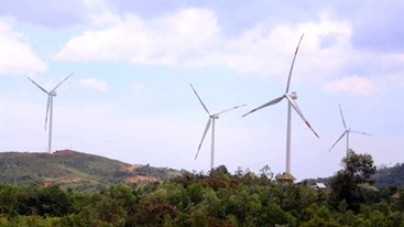
 The Ministry of Industry and Trade requests government agencies to coordinate in organizing Earth Hour 2024
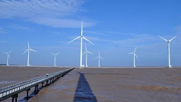
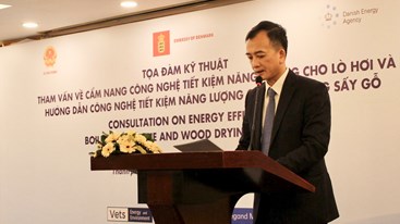 Consultation on Energy Efficiency Boiler Catalogue and Wood Drying Guideline
.png?w=367&h=206&mode=crop) Request for expression of interest - C2.1.13: Capacity Building on energy efficiency policies development
Request for expression of interest - C2.1.13: Capacity Building on energy efficiency policies development
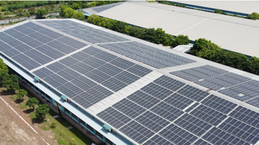 Son Ha Co., Ltd, applies energy efficiency and conservation measures
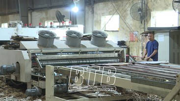 Phuc Kien Co., Ltd., is effectively implementing energy-saving measures
 Request for expression of interest - C2.1.12: Independent monitoring of safeguards implementation


.jpg?w=367&h=206&mode=crop)